欢迎访问《电化学(中英文)》期刊官方网站,今天是

电化学(中英文) ›› 2024, Vol. 30 ›› Issue (3): 2305251.  doi: 10.13208/j.electrochem.2305251

• 快讯 • 上一篇    下一篇

单层石墨烯微米尺度图案化和功能化:调控电子传输特性

崔苗苗a, 韩联欢a,b,*(), 曾兰平a, 郭佳瑶a, 宋维英a, 刘川a, 吴元菲a, 罗世翊a, 刘云华c,*(), 詹东平a,*()   

  1. a厦门大学化学化工学院化学系,固体表面物理化学国家重点实验室,电化学技术教育部工程研究中心,福建 厦门 361005
    b厦门大学萨本栋微纳米科学与技术研究所机电工程系,福建 厦门 361005
    c华中科技大学国家CAD支撑软件工程研究中心,湖北 武汉 430074
  • 收稿日期:2023-05-25 修回日期:2023-07-05 接受日期:2023-07-14 出版日期:2024-03-28 发布日期:2023-09-25

Micropatterning and Functionalization of Single Layer Graphene: Tuning Its Electron Transport Properties

Cui Miao-Miaoa, Han Lian-Huana,b,*(), Zeng Lan-Pinga, Guo Jia-Yaoa, Song Wei-Yinga, Liu Chuana, Wu Yuan-Feia, Luo Shi-Yia, Liu Yun-Huac,*(), Zhan Dong-Pinga,*()   

  1. aDepartment of Chemistry, College of Chemistry and Chemical Engineering, State Key Laboratory of Physical Chemistry of SolidSurfaces (PCOSS), Engineering Research Center of Electrochemical Technologies of Ministry of Education, Xiamen University,Xiamen 361005, China
    bDepartment of Mechanical and Electrical Engineering, Pen-Tung Sah Institute of Micro-Nano Science and Technology, Xiamen University; Xiamen 361005, China
    cNational CAD Support Software Engineering Research Center Huazhong University of Science and Technology, Wuhan 430074, China
  • Received:2023-05-25 Revised:2023-07-05 Accepted:2023-07-14 Published:2024-03-28 Online:2023-09-25
  • Contact: *Tel: (86-592)18638012492, E-mail: hanlianhuan@xmu.edu.cn;Tel: (86)13071265596, E-mail: liuyh@mail.hust.edu.cn;Tel: (86-592)2185797, E-mail: dpzhan@xmu.edu.cn

摘要:

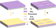
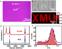
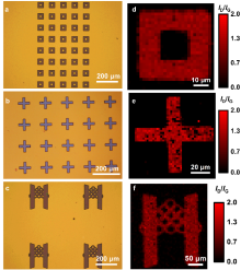
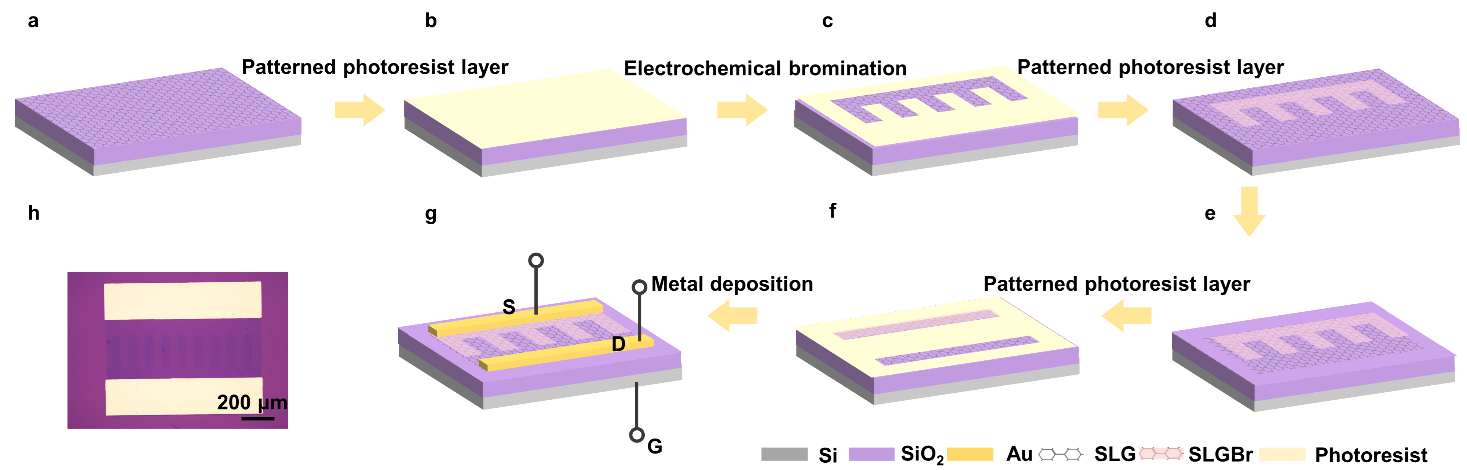
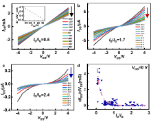
石墨烯具有优异的物理特性,如单原子厚度、极高的载流子迁移率等。然而,其零带隙的半金属特性限制了其在高性能场效应晶体管中的应用。为此,研究者们提出了石墨烯纳米化、外场诱导、掺杂以及化学图案化等策略,以调控其带隙宽度。但是,这些方法的可控性以及稳定性还需要进一步改善。在本研究中,我们提出采用电化学溴化并结合光刻图案化调控单层石墨烯的电子传输特性,通过这种方法,成功制备了图案化的溴化石墨烯(SLGBr)。进一步研究表明,单层石墨烯的电子传输性能可以通过溴化程度来调控。当溴化程度较小时,SLGBr表现为电阻特性,且其电导随溴化程度增加而减小;当溴化程度增加到一定值时,SLGBr表现为与半导体类似的特性。本研究将为全石墨烯器件的制备提供可行的技术路线,拓展其在微电子领域的应用。

关键词: 石墨烯图案化, 电子传输, 电化学溴化, 光刻, 全石墨烯器件

Abstract:

As a promising 2D material, graphene exhibits excellent physical properties including single-atom-scale thickness and remarkably high charge carrier mobility. However, its semi-metallic nature with a zero bandgap poses challenges for its application in high-performance field-effect transistors (FETs). In order to overcome these limitations, various approaches have been explored to modulate graphene's bandgap, including nanoscale confinement, external field induction, doping, and chemical micropatterning. Nevertheless, the stability and controllability still need to be improved. In this study, we propose a feasible method that combines electrochemical bromination and photolithography to precisely tune the electron transport properties of single layer graphene (SLG). Through this method, we successfully fabricated various brominated SLG (SLGBr) micropatterns with high accuracy. Futher investigation revealed that the electron transport properties of SLG can be conveniently tuned by controlling the degree of bromination. The SLGBr exhibited a resistance, and have a decreasing conductance with the bromination degree increasing. When the bromination degree increased to a critical value, the SLGBr demonstrated semiconducting characteristics. This research offers a prospective route for the fabrication of graphene-based devices, providing potential applications in the realm of microelectronics.

Key words: Graphene patterning, Electron transport, Electrochemical bromination, Photolithography, All graphene device