应用于大马士革工艺的纳米孪晶铜脉冲电沉积研究
收稿日期: 2022-09-23
修回日期: 2022-11-23
录用日期: 2022-12-02
网络出版日期: 2022-12-08
Pulse Electroplating of Nanotwinned Copper Using MPS-PEG Two-Additive System for Damascene via Filling Process
Received date: 2022-09-23
Revised date: 2022-11-23
Accepted date: 2022-12-02
Online published: 2022-12-08
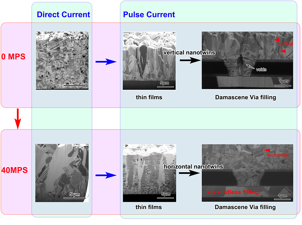
本文在前期优化的电镀液的基础上,使用脉冲电镀工艺获得了高密度的纳米孪晶铜。为了进一步揭示孪晶形成的影响因素,研究了系列MPS浓度在镀液中的作用。当镀液中并未添加MPS时,镀层由粗大的晶粒组成,平均晶粒大小为0.9 μm,晶粒内部含有少量的垂直或倾斜于膜面的孪晶界,镀层的晶粒取向为(110)和(111)共存,两者织构比例分别为49%和27.8%。从FIB微观组织观察和X射线衍射的结果可知,当镀液中添加10 ppm的MPS后,镀层组织变为柱状纳米孪晶铜组织,柱状晶内部含有高密度水平方向的孪晶界,同时晶粒取向变为高度择优的(111)。当MPS含量从10 ppm持续上升至40 ppm,镀层组织和晶粒取向无明显变化。具体地,当镀液中添加40 ppm的MPS时,镀层晶粒大小为0.6 μm,且镀层晶粒(110)和(111)的织构比例分别为3.45%和95.1%。这说明,可以通过MPS的含量调节提高纳米孪晶铜电镀液的填充能力,而纳米孪晶微观组织的形成并不受影响。基于上述结果,我们使用该电镀液配方及工艺进行了大马士革微盲孔的填充。结果表明,当MPS含量为40 ppm时,可以实现大马士革微盲孔的无孔填充。纳米孪晶铜电镀液填充能力的提升使得纳米孪晶铜在IC制造应用成为可能,很大程度上促进了下一代互连材料的发展。
王玉玺 , 高丽茵 , 万永强 , 李哲 , 刘志权 . 应用于大马士革工艺的纳米孪晶铜脉冲电沉积研究[J]. 电化学, 2023 , 29(8) : 2209231 . DOI: 10.13208/j.electrochem.2209231
High density nanotwinned copper films were pulse electroplated using an optimized electrolyte. In order to find out the influencing factors on the formation of nanotwins, series contents of MPS were added to the electrolyte during the pulse electroplating process. It was found that the copper films electroplated without MPS had large grains but a few nanotwins. And the grain size was about 0.9 μm on average, and the texture components of (110) and (111) crystal orientations were calculated as 49% and 27.8%, respectively. Differently, when 10 ppm MPS was added, the microstructure was changed to columnar grain with high density of horizontal nanotwins and the crystal orientation was also changed to highly (111) orientated one. However, when the MPS content was continuously increased from 10 ppm to 40 ppm, the microstructure and crystal orientation were almost unchanged as detected by the secondary ion microscopy of focus ion beam and X ray diffraction. Specifically, when 40 ppm MPS was used, the average grain size was 0.6 μm, and the texture components of (110) and (111) crystal orientations were 3.45% and 95.1%, respectively. It demonstrated that the nanotwinned copper can be electroplated at a large concentration range of MPS, which also meant that the filling ability of nanotwinned copper electrolyte could be adjusted by MPS content without influencing the microstructure. Finally, these electrolytes with different contents of MPS were used in the Damascene via filling. The results showed that when the content of MPS was 40 ppm, the Damascus via was completely filled without voids. The achievement of via filling with nanotwinned copper makes the application of nanotwinned copper possible in Integrated Circuit (IC) fabrication, which also greatly promotes the development of interconnected material for next generation.
Key words: pulse electroplating; nanotwinned copper; via filling; Damascene process
[1] | Cho D H, Seo S M, Kim J B, Rajendran S H, Jung J P. A review on the fabrication and reliability of three-dimensional integration technologies for microelectronic packaging: Through-Si-Via and solder bumping process[J]. Metals, 2021, 11(10): 1664. |
[2] | Tu K N. Reliability challenges in 3D IC packaging technology[J]. Microelectron. Reliab., 2011, 51(3): 517-523. |
[3] | Shen Y, Li B B, Ma Y, Wang Z L. Research progress in electroless cobalt plating and the bottom-up filling of electroless plating[J]. J. Electrochem., 2022, 28(7): 2213002. |
[4] | Tan B Z, Liang J L, Lai Z L, Luo J Y. Electrochemical deposition of copper pillar bumps with high uniformity[J]. J. Electrochem., 2022, 28(7): 2213004. |
[5] | Lu L, Shen Y F, Chen X H, Qian L H, Lu K. Ultrahigh strength and high electrical conductivity in copper[J]. Science, 2004, 304(5669): 422-426. |
[6] | Tseng C H, Tu K N, Chen C. Comparison of oxidation in uni-directionally and randomly oriented cu films for low temperature Cu-to-Cu direct bonding[J]. Sci. Rep., 2018, 8(1): 1-7. |
[7] | Sun F L, Liu Z Q, Li C F, Zhu Q S, Zhang H, Suganuma K. Bottom-up electrodeposition of large-scale nanotwinned copper within 3D through silicon via[J]. Materials, 2018, 11(2): 319. |
[8] | Huang J, Gao L Y, Peng Z J, Li Z, Liu Z Q, Sun R. Effect of sodium thiazolinyl dithiopropane sulphonate (SH110) addition on electroplating nanotwinned copper films and their filling performance of fine-pitch redistributed layer (RDL)[J]. Nanotechnology, 2023, 34(1): 015710. |
[9] | Dong M Y, Chen P X, Hang T, Li M. Nanotwinned copper micro-cone array fabricated by pulse electrodeposition for low-temperature bonding - sciencedirect[J]. Materials Letters, 290: 129470. |
[10] | Bai Y, Hu H, Ling H Q, Hang T, Hu A M, Wu Y M, Li M. Communication—fabrication of vertical nanotwinned copper with (220) texture by direct current electrodeposition[J]. J. Electrochem. Soc., 2021, 168(8): 082506. |
[11] | Li Y J, Tu K N, Chen C. Tensile properties and thermal stability of unidirectionally< 111>-oriented nanotwinned and< 110>-oriented microtwinned copper[J]. Materials, 2020, 13(5): 1211. |
[12] | Zhu Q S, Zhang X, Li S J, Liu C Z, Li C F. Communication—electrodeposition of nano-twinned Cu in void-free filling for blind microvia of high density interconnect[J]. J. Electrochem. Soc., 2019, 166(1): D3097-D3099. |
[13] | Zhan X F, Lian J, Li H J, Wang X B, Zhou J A, Trieu K, Zhang X P. Preparation of highly (111) textured nanotwinned copper by medium-frequency pulsed electrodeposition in an additive-free electrolyte[J]. Electrochim. Acta, 2020, 365: 137391. |
[14] | Hai N T M, Huynh T T M, Fluegel A, Arnold M, Mayer D, Reckien W, Bredow T, Broekmann P. Competitive anion/anion interactions on copper surfaces relevant for damascene electroplating[J]. Electrochim. Acta, 2012, 70: 286-295. |
[15] | Zhang Y B, Gao L Y, Li X, Li Z, Ma X L, Liu Z Q, Sun R. Electroplating nanotwinned copper for ultrafine pitch redistribution Layer (RDL) of advanced packaging technology. In: 2021 22nd International Conference on Electronic Packaging Technology (ICEPT): IEEE, 2021. 1-6. |
[16] | Du L, Shi T L, Su L, Xue D M, Liao G L. A novel bottom-up copper filling of blind silicon vias in 3d electronic packaging[J]. J. Micromech. Microeng., 2015, 25(4): 045005. |
[17] | Zhou Z H, Tan C L, Xiong W, Xi D L, Liu B Y. Introduction of development and application technology of organic additives for acid copper electroplating[J]. J. Electrochem., 2022, 28(6): 2104531. |
[18] | Meng Y C, Zhou M M, Huang W, Min Y L, Shen X X, Xu Q J. Benzyl-containing quaternary ammonium salt as a new leveler for microvia copper electroplating[J]. Electrochim. Acta, 2022, 429: 141013. |
[19] | Zhou M M, Meng Y C, Ling J W, Zhang Y, Huang W, Min Y L, Shen X X, Xu Q J. 5-Amino-1,3,4-Thiadiazole-2-Thiol as a new leveler for blind holes copper electroplating: Theoretical calculation and electrochemical studies[J]. Applied Surface Science, 2022, 606: 154871. |
[20] | Chen Q W, Wang Z Y, Cai J, Liu L T. The influence of ultrasonic agitation on copper electroplating of blind-vias for soi three-dimensional integration[J]. Microelectron. Eng., 2010, 87(3): 527-531. |
[21] | Tao Z H, Long Z Y, Tengxu L J, Liu G T, Tao X F. The synergistic effects of additives on the micro vias copper filling[J]. J. Electroanal. Chem., 2022: 116456. |
[22] | Huang J, Gao L Y, Liu Z Q. The electrochemical behavior of leveler JGB during electroplating of nanotwinned copper[C]// 2020 21st International Conference on Electronic Packaging Technology (ICEPT):IEEE, 2020: 1-4. |
[23] | Sun F L, Gao L Y, Liu Z Q, Zhang H, Sugahara T, Nagao S, Suganuma K. Electrodeposition and growth mechanism of preferentially orientated nanotwinned Cu on silicon wafer substrate[J]. J. Mater. Sci. Technol., 2018, 34(10): 1885-1890. |
[24] | Li Z G, Gao L Y, Li Z, Sun R, Liu Z Q. Regulating the orientation and distribution of nanotwins by trace of gelatin during direct current electroplating copper on titanium substrate[J]. J. Mater. Sci., 2022, 57(37): 17797-17811. |
[25] | Wang Y X, Gao L Y, Wan Y Q, Liu Z Q, Sun R. Effect of pulse off time on microstructure and properties of twinned copper films by pulse electrodeposition[C]// . 2022 23rd International Conference on Electronic Packaging Technology (ICEPT), Dalian, China, 2022: 1-5. |
[26] | Chan T C, Lin Y M, Tsai H W, Wang Z M, Liao C N, Chueh Y L. Growth of large-scale nanotwinned Cu nanowire arrays from anodic aluminum oxide membrane by electrochemical deposition process: Controllable nanotwin density and growth orientation with enhanced electrical endurance performance[J]. Nanoscale, 2014, 6(13): 7332-7338. |
[27] | Hsiao H Y, Liu C M, Lin H W, Liu T C, Lu C L, Huang Y S, Chen C, Tu K N. Unidirectional growth of microbumps on (111)-oriented and nanotwinned copper[J]. Science, 2012, 336(6084): 1007-1010. |
[28] | Pavithra C L P, Sarada B V, Rajulapati K V, Ramakrishna M, Gundakaram R C, Rao T N, Sundararajan G. controllable crystallographic texture in copper foils exhibiting enhanced mechanical and electrical properties by pulse reverse electrodeposition[J]. Cryst. Growth Des., 2015, 15(9): 4448-4458. |
[29] | Xu D, Kwan W L, Chen K, Zhang X, Ozolins V, Tu K N. Nanotwin formation in copper thin films by stress/strain relaxation in pulse electrodeposition[J]. Appl. Phys. Lett., 2007, 91(25): 254105. |
[30] | Marro J B, Darroudi T, Okoro C A, Obeng Y S, Richardson K C. The influence of pulse plating frequency and duty cycle on the microstructure and stress state of electroplated copper films[J]. Thin Solid Films, 2017, 621: 91-97. |
[31] | Wang C, Zhang J Q, Yang P X, An M Z. Through-hole filling by copper electroplating using sodium thiazolinyl-dithiopropane sulfonate as the single additive[J]. Int. J. Electrochem. Sci., 2012, 7(11): 10644-10651. |
[32] | Hong B, Jiang C H, Wang X J. Influence of complexing agents on texture formation of electrodeposited copper[J]. Surf. Coat Technol., 2007, 201(16-17): 7449-7452. |
/
〈 |
|
〉 |