高深径比通孔脉冲电镀添加剂及电镀参数的优化
收稿日期: 2022-02-28
修回日期: 2022-04-20
网络出版日期: 2022-05-24
基金资助
国家自然科学基金项目(21878029);国家自然科学基金项目(21706195);国家自然科学基金项目(21676035);广东省“扬帆计划”先进印制电路关键技术研发及产业化项目(2015YT02D025)
Optimization of Pulse Plating Additives and Plating Parameters for High Aspect Ratio Through Holes
Received date: 2022-02-28
Revised date: 2022-04-20
Online published: 2022-05-24
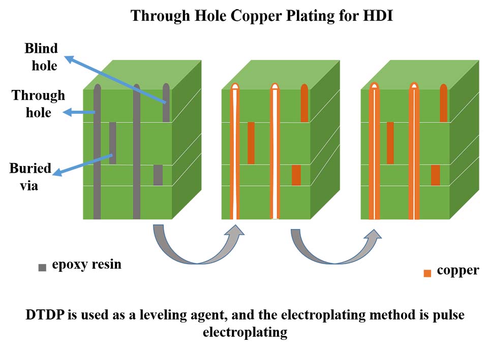
本文采用毒性小,价格低廉的2, 2′-二硫代二吡啶(2, 2′-Dithiodipyridine,DTDP)作为通孔电镀铜添加剂,对添加剂体系的浓度及脉冲电镀参数进行了优化。首先,对DTDP能否在高深径比通孔脉冲电镀过程中起到整平作用进行探究,并对包含其在内的四种添加剂的浓度进行正交优化,得到了当电镀效果较好时的最优添加剂浓度,但是该条件电镀后的通孔呈“狗骨状”。其次再利用正交优化后的电镀液,采用单因素分析法对脉冲电镀参数进行优化,得出此时较优的脉冲电镀参数,并消除上述通孔“狗骨”现象。在电镀试验后,通过采用扫描电子显微镜(SEM)和浸锡热应力实验对电镀后的实验板进行性能测试。
杨凯 , 陈际达 , 陈世金 , 许伟廉 , 郭茂桂 , 廖金超 , 吴熷坤 . 高深径比通孔脉冲电镀添加剂及电镀参数的优化[J]. 电化学, 2022 , 28(6) : 2104491 . DOI: 10.13208/j.electrochem.210449
As an important component in electronic products, printed circuit board (PCB) plays a supporting and interconnecting role for the electronic components in it. With the development of communication technology, electronic products are developing in the direction of “thin, light and small”, and high density interconnection (HDI) comes into being. Due to the high-density interconnection characteristics of HDI boards, the thickness of the board is increasing. At the same time, in order to reserve space for the laying of fine lines on the subsequent board surface, the diameter of the through holes on the board is also decreasing, so the depth-diameter ratio of the through holes is increasing. In order to ensure the electrical interconnection between the middle layers of the HDI board, the through-hole plating technology has become the key. In the process of through-hole electroplating, due to the relatively small diameter of the through-hole, the current density distribution inside and outside the hole is uneven, and the dispersion ability of the plating solution is poor, resulting in uneven copper plating layer and thick surface copper layer, which is not conducive to subsequent fine circuits laying. An effective way to overcome this drawback is to add electroplating additives to the bath, and to use bidirectional pulse electroplating technology. Therefore, 2, 2'-dithiodipyridine (DTDP) with low toxicity and low cost was used as an additive in the plating solution, and its application in pulse plating of high aspect ratio through holes was studied. The additive concentration and pulse plating parameters were optimized. It was concluded that DTDP could be applied to pulse plating of high aspect ratio through holes. And through orthogonal optimization experiments, the optimal concentration of additives suitable for the high aspect ratio (14.5:1) through-hole electroplating was obtained. Finally, the throwing power of the plating solution was measured at about 86%, and the average thickness of surface copper was about 38 μm. It is not conducive to the operation of the subsequent process, and the through hole is in the shape of a “dog bone”; then the single factor analysis of the pulse parameters was carried out, and finally, the optimal single-stage pulse plating parameters were obtained. At this time, the throwing power of the plating solution was about 75%, and the average thickness of the surface copper was about 27.6 μm, which is convenient for the subsequent processing and solves the above-mentioned “dog bone” phenomenon. SEM test and tin immersion thermal stress test were performed on the experimental boards of the two experiments separately. The SEM images found that the coating particles of the two experimental boards were fine and uniform, and relatively flat; the tin immersion thermal stress test results did not find any cracks. These phenomena are all in line with industry requirements, so it provides a certain basis for the research of high aspect ratio through-hole pulse electroplating. Further experiments are needed in the follow-up to make the plating solution higher in throwing power and at the same time reduce the surface copper thickness.
Keywords: plating additive; pulse electroplating; high aspect ratio through hole; orthogonal design tests; throwing power
[1] | Ikram M, Sultan K, Lateef M F, Alqadami A S M. A road towards 6G communication-A review of 5G antennas, arrays, and wearable devices[J]. Electronics, 2022, 11(1): 169. |
[2] | Zhang Y H, An M Z, Yang P X, Zhang J Q. Recent advances in electroplating of through-hole copper interconnection[J]. Electrocatalysis, 2021, 12(6): 619-627. |
[3] | Potelon T, Ettorre M, Le Coq L, Bateman T, Francey J. Sauleau R. Reconfigurable CTS antenna fully integrated in PCB technology for 5G backhaul applications[J]. IEEE Trans. Antennas Propag., 2019, 67(6): 3609-3618. |
[4] | Novak M H, Miranda F A, Volakis J L. Ultra-wideband phased array for millimeter-wave ISM and 5G bands, realized in PCB[J]. IEEE Trans. Antennas Propag., 2018, 66(12): 6930-6938. |
[5] | Xiao N(肖宁). Study on microvia filling preformances and action mechanisms of epe inhibitors in copper electroplating processepe[D]. Harbin: Institute of Technology(哈尔滨工业大学), 2013. |
[6] | Wang H X(王慧秀), He W(何为), He B(何波), Long H R(龙海荣). Current situation and development prospects of high density interconnection printed circuit board technology[J]. World Sci.-Tech. R & D (世界科技研究与发展), 2006, 4: 14-18. |
[7] | Jones T D A, Bernassau A, Flynn D, Price D, Beadel M, Desmulliez M P Y. Copper electroplating of PCB interconnects using megasonic acoustic streaming[J]. Ultrason. Sonochem., 2018, 42: 434-444. |
[8] | Wang Z Y(王赵云), Jin L(金磊), Yang J Q(杨家强), Li W Q(李威青), Zhan D P(詹东平), Yang F Z(杨防祖), Sun S G(孙世刚). Studies and progresses on hole metallization in high-density interconnected printed circuit boards[J]. J. Electrochem.(电化学), 2021, 27(3): 316-331. |
[9] | Takagi K, Honma H, Sasabe T. Development of sequential build-up multilayer printed wiring boards in japan[J]. IEEE Electr. Insul. Mag., 2003, 19(5): 27-56. |
[10] | Zhang J(张佳). Application research on plating throwing power for printed circuit boards based on minitab software[D]. Chengdu: University of Electronic Science and Technology(电子科技大学), 2012. |
[11] | Broekmann P, Fluegel A, Emnet C, Arnold M, Roeger-Goepfert C, Wagner A, Hai N T M, Mayer D. Classification of suppressor additives based on synergistic and antagonistic ensemble effects[J]. Electrochim. Acta, 2011, 56(13): 4724-4734. |
[12] | Li Y B, Wang W, Li Y L. Adsorption behavior and related mechanism of Janus Green B during copper via-filling process[J]. J. Electrochem. Soc., 2009, 156(4): D119-D124. |
[13] | Shen S Y(沈世玉). Studies on the influence of JGB, PEG and Cl- additives on copper electrodeposition[D]. Chongqing: Chongqing University(重庆大学), 2014. |
[14] | Wang X(王旭), Zhang S T(张胜涛), Chen S J(陈世金), Guo H L(郭海亮), Wen Y N(文亚男), Tan B C(谭博川), Wang Y(王亚). Optimization of additives for copper electroplating of through holes with a high aspect ratio[J]. Electroplating & Finishing(电镀与涂饰), 2020, 39(8): 461-468. |
[15] | Wang X(王旭), Zhang S T(张胜涛), Chen S J(陈世金), Guo H L(郭海亮), Luo J Y(罗佳玉), Wen Y N(文亚男), Guo M G(郭茂桂), Xu W L(许伟廉). Optimization of additives for copper electroplating of through holes on printed circuit board[J]. Electroplating & Finishing(电镀与涂饰), 2019, 38(15): 780-786. |
[16] | Chandrasekar M.S. Pushpavanam M. Pulse and pulse reverse plating-Conceptual, advantages and applications[J]. Electrochimica Acta, 2008, 53(8): 3313-3322. |
[17] | Yung K C, Chan K C, Yue T M, Yeung K F. The effect of waveform for pulse plating on copper plating distribution of microvia in PCB manufacture[J]. Int. J. Adv. Manuf. Technol., 2004, 23(3-4): 245-248. |
[18] | Marro J B, Darroudi T, Okoro C A, Obeng Y S, Richardson K C. The influence of pulsed electroplating frequency and duty cycle on copper film microstructure and stress state[J]. Thin solid films, 2017, 621: 91-97. |
[19] | Shen F Y, Dow W P, Liu A H, et al. Periodic pulse reverse Cu plating for through-hole filling[J]. ECS Electrochem. Lett., 2013, 2(5): D23-D25. |
[20] | Chen X L(陈雪丽), Wang C(王翀), He W(何为), Zhang W H(张伟华), Chen Y M(陈苑明), Tao Y G(陶应国). Application of periodic pulse reverse plating for through hole interconnection of communication backplane board[J]. Printed Circuit Info.(印制电路资讯), 2021, 29(5): 7-11. |
[21] | Reid J. Copper electrodeposition: Principles and recent progress[J]. Jpn. J. Appl. Phys. Part 1 - Regul. Pap. Short Notes Rev. Pap., 2001, 40(4B): 2650-2657. |
[22] | Dela Pena E M, Roy S. Electrochemical effect of copper gleam additives during copper electrodeposition[J]. Trans. Inst. Metal Finish., 2017, 95(3): 158-164. |
/
〈 |
|
〉 |