欢迎访问《电化学(中英文)》期刊官方网站,今天是
综述

玻璃通孔三维互连镀铜填充技术发展现状

  • 纪执敬 ,
  • 凌惠琴 ,
  • 吴培林 ,
  • 余瑞益 ,
  • 于大全 ,
  • 李明
展开
  • 1.上海交通大学材料科学与工程学院,上海 200240
    2.厦门云天半导体科技有限公司,福建 厦门 361026
    3.厦门大学电子科学与技术学院,福建 厦门 361104
*李明: Tel: (86-21)34202542, E-mail: mingli90@sjtu.edu.cn;
于大全:Tel: (86-592)2188342, E-mail: yudaquan@xmu.edu.cn

收稿日期: 2021-11-08

  修回日期: 2022-01-21

  网络出版日期: 2022-03-04

Development Status of Copper Electroplating Filling Technology in Through Glass Via for 3D Interconnections

  • Zhi-Jing Ji ,
  • Hui-Qin Ling ,
  • Pei-Lin Wu ,
  • Rui-Yi Yu ,
  • Da-Quan Yu ,
  • Ming Li
Expand
  • 1. School of Materials Science and Engineering, Shanghai Jiao Tong University, Shanghai 200240, China
    2. Xiamen Sky Semiconductor Co., Ltd., Xiamen 361026, China
    3. School of Electronic Science and Engineering, Xiamen University, Xiamen 361104, China

Received date: 2021-11-08

  Revised date: 2022-01-21

  Online published: 2022-03-04

摘要

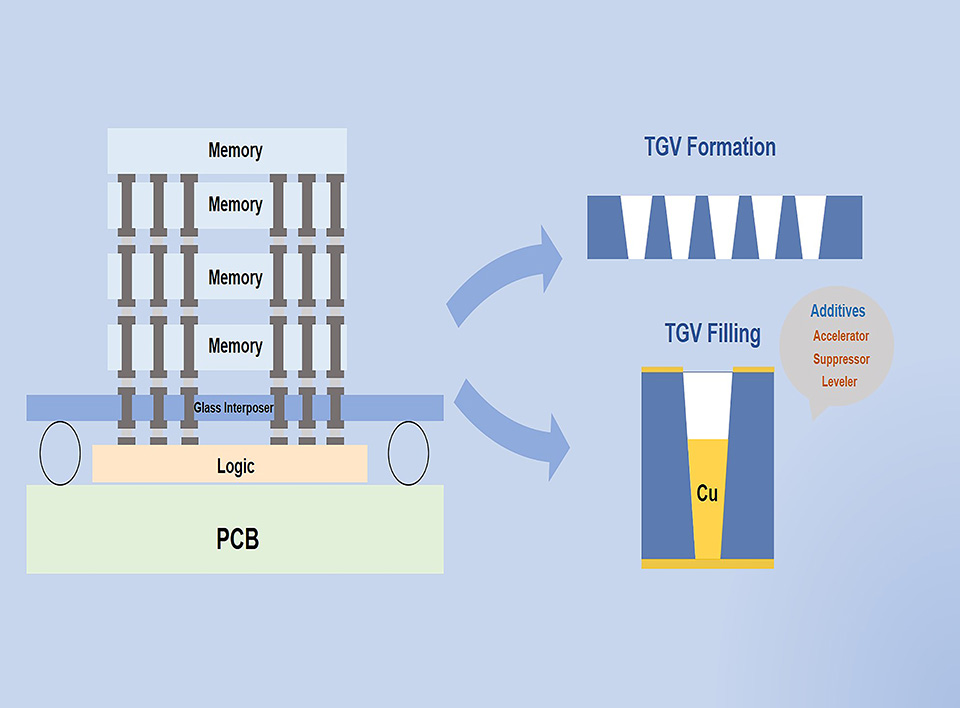
随着摩尔定律的发展迟缓,微电子器件的高密度化、微型化对先进封装技术提出了更高的要求。中介层技术作为2.5D/3D封装中的关键技术,受到了广泛研究。按照中介层材料不同,主要分为有机中介层、硅中介层以及玻璃中介层。与硅通孔(through silicon via, TSV)互连相比,玻璃通孔(through glass via,TGV)中介层(interposer)因其具有优良的高频电学特性、 工艺简单、 成本低以及可调的热膨胀系数(coefficient of thermal expansion,CTE)等优点,在2.5D/3D先进封装领域受到广泛关注。然而玻璃的导热系数(约1 W·m-1·K-1)与硅(约150 W·m-1·K-1)相比要低很多,因此玻璃中介层存在着严重的散热问题。为得到高质量的TGV中介层,不仅需要高效低成本的通孔制备工艺,还需要无缺陷的填充工艺,目前玻璃中介层面临的挑战也主要集中在这两方面。本文首先介绍了TGV的制备工艺,如超声波钻孔(ultra-sonic drilling, USD)、超声波高速钻孔(ultra-sonic high speed drilling,USHD)、湿法刻蚀、深反应离子刻蚀(deep reactive ion etching, DRIE)、光敏玻璃、激光刻蚀、激光诱导深度刻蚀(laser induced deep etching, LIDE)等。接着围绕TGV的无缺陷填充进行总结,概述了TGV的几种填充机理以及一些填充工艺,如bottom-up填充、蝶形填充以及conformal填充。然后对TGV电镀添加剂的研究进展进行了介绍,包括典型添加剂的作用机理以及一些新型添加剂的研究现状,最后并对TGV实际应用情况进行了简要综述。

本文引用格式

纪执敬 , 凌惠琴 , 吴培林 , 余瑞益 , 于大全 , 李明 . 玻璃通孔三维互连镀铜填充技术发展现状[J]. 电化学, 2022 , 28(6) : 2104461 . DOI: 10.13208/j.electrochem.210446

Abstract

With the slow development of Moore's Law, the high density and miniaturization of microelectronic devices put forward higher requirements for advanced packaging technology. As a key technology in 2.5D/3D packaging, interposer technology has been extensively studied. According to different interposer materials, it is mainly divided into organic interposer, silicon interposer and glass interposer. Compared with the through silicon via (TSV) interconnection, the through glass via (TGV) interposer has received extensive attention in the 2.5D/3D advanced packaging field for its advantages of excellent high-frequency electrical characteristics, simple process, low cost, and adjustable coefficient of thermal expansion (CTE). However, the thermal conductivity of glass (about 1 W·m-1·K-1) is much lower than that of silicon (about 150 W·m-1·K-1), thus, the glass interposer has serious heat dissipation problems. In order to obtain a high-quality TGV interposer, not only an efficient and low-cost via preparation process, but also a defect-free filling process is required. The challenges faced by glass interposer is mainly concentrated in these two aspects. This review firstly introduces the preparation process of TGV, such as ultra-sonic drilling (USD), ultra-sonic high speed drilling (USHD), wet etching, deep reactive ion etching (DRIE), photosensitive glass, laser etching, laser induced deep etching (LIDE), etc. Then it summarizes the defect-free filling of TGV, and outlines several filling mechanisms and some current filling processes of TGV, such as bottom-up filling mechanisms, butterfly filling mechanisms and conformal filling mechanisms. Among the filling mechanisms of the above three filling methods, the filling method of bottom-up is the most studied one, and many scholars have given relevant explanations. Currently, the main ones that are commonly used are the diffusion-consumption mechanism, curvature enhanced adsorbate coverage mechanism (CEAC), convection dependent adsorption mechanism (CDA), and S-shaped negative differential resistance theory. In the process of TGV filling, the type and concentration of base bath, additives and electroplating process will affect the filling status of TGV. At present, the constant current plating mode is most commonly used in the process of TGV filling. Then the research progress of TGV electroplating additives is introduced, including the action mechanism of typical additives and the current research status of some new additives. Through glass via technology can be filled with the synergistic action of accelerators, suppressors and levelers. Finally, the practical application of TGV is briefly reviewed, for example, glass interposer is used in 3D integrated passive device (IPD), embedded glass fan-out technology (eGFO), integrated antenna packaging, micro-electro-mechanical system (MEMS), multi-chip module packaging, as well as the applications in the field of optical integration technology.

参考文献

[1] Sukumaran V, Kumar G, Ramachandran K, Suzuki Y, Demir K, Sato Y, Seki T, Sundaram V, Tummala R R. Design, fabrication, and characterization of ultrathin 3-D glass interposers with through-package-vias at same pitch as TSVs in silicon[J]. IEEE Trans. Compon. Pack. Manuf. Technol., 2014, 4(5): 786-795.
[2] Hsieh M C, Kang K T, Choi H C, Kim Y C. International Microsystems Packaging Assembly and Circuits Technology Conference, Taipei, October 26-28, 2016[C]. Piscataway: IEEE, 2016.
[3] Hsieh M, Lin S, Hsu I, Chen C Y, Cho N J. 2017 21st European Microelectronics and Packaging Conference (EMPC) & Exhibition, Warsaw, September 10-13, 2017[C]. Piscataway: IEEE, 2018.
[4] Usman A, Shah E, Satishprasad N B, Chen J L, Bohlemann S A, Shami S H, Eftekhar A A, Adibi A. Interposer technologies for high-performance applications[J]. IEEE Trans. Compon. Pack. Manuf. Technol., 2017, 7(6): 819-828.
[5] Kuramochi S, Kudo H, Akazawa M, Mawatari H, Tanaka M, Fukuoka Y. 2016 6th Electronic System-Integration Technology Conference (ESTC), Grenoble, September 13-15, 2016[C]. Piscataway: IEEE, 2016.
[6] Kuramochi S, Koiwa S, Nagano H, Iida J, Akazawa M, Mawatari H, Suzuki K, Fukuoka Y. 2016 Pan Pacific Microelectronics Symposium (Pan Pacific), Big Island, HI, January 25-28, 2016[C]. Piscataway: IEEE, 2016.
[7] Ohtsuki C, Kokubo T, Yamamuro T. Mechanism of apatite formation on CaO-SiO2-P2O5 glasses in a simulated body fluid[J]. J. Non-Cryst. Solids, 1992, 143(1): 84-92.
[8] Töpper M, Ndip I, Erxleben R, Brusberg L, Nissen N, Schröder H, Yamamoto H, Todt G, Reichl H. 2010 Proceedings 60th Electronic Components and Technology Conference, Las Vegas, NV, June 1-4, 2010[C]. Piscataway: IEEE, 2010.
[9] Ogutu P G. Hybrid metallization of glass and superconformal filling of through glass vias for interposer application[D]. Binghamton: State University of New York at Binghamton, 2015.
[10] Sukumaran V, Bandyopadhyay T, Sundaram V, Tummala R. Low-cost thin glass interposers as a superior alternative to silicon and organic interposers for packaging of 3-D ICs[J]. IEEE Trans. Compon. Pack. Manuf. Technol., 2012, 2(9): 1426-1433.
[11] Garrou P, Koyanagi M, Ramm P. Handbook of 3D integration: volume 3-3D process technology[M]. Germany: Wiley-VCH Verlag GmbH & Co. KGaA, 2014.
[12] Wang Q W(王强文), Guo Y H(郭育华), Liu J J(刘建军), Wang Y L(王运龙). High heat dissipation performance of the TGV interposer[J]. Micronanoelectron. Technol.(微纳电子技术), 2021, 58(2): 177-183.
[13] Zheng L, Zhang Y, Zhang X, Bakir M S. 2015 IEEE 65th Electronic Components and Technology Conference, San Diego, CA, May 26-29, 2015[C]. Piscataway: IEEE, 2015.
[14] Lai W C, Chuang H H, Tsai C H, Yeh E H, Lin C H, Peng T H, Yen L J, Liao W S, Hung J N, Sheu C C, Yu C H, Wang C T, Yee K C, Yu D. 2013 IEEE International Electron Devices Meeting, Washington, DC, December 9-11, 2013[C]. Piscataway: IEEE, 2014.
[15] LPKF. Through glass via (TGV) wafer[EB/OL]. (2018-02-05). https://www.vitrion.com/en/applications/through-glass-vias-tgv/
[16] Ostholt R, Ambrosius N, Kruger R A. Proceedings of the 5th Electronics System-integration Technology Conference (ESTC), Helsinki, September 16-18, 2014[C]. Piscataway: IEEE, 2014.
[17] Shacham-Diamand Y, Osaka T, Datta M, Ohba T. Advanced nanoscale ULSI interconnects: Fundamentals and applications[M]. New York: Springer, 2009.
[18] Su W, Yao L B, Yang F, Li P Y, Chen J, Liang L F. Electroless plating of copper on surface-modified glass substrate[J]. Appl. Surf. Sci., 2011, 257(18): 8067-8071.
[19] Huang T, Sundaram V, Raj P M, Sharma H, Tummala R. 2014 IEEE 64th Electronic Components and Technology Conference (ECTC), Orlando, FL, May 27-30, 2014[C]. Piscataway: IEEE, 2014.
[20] Xie D(谢迪), Li H(李浩), Wang C X(王从香), Cui K(崔凯), Hu Y F(胡永芳). Study on technology of through glass via for 3D integration package[J]. Electronics & Packaging(电子与封装), 2021, 21(7): 20-25.
[21] Wang B K, Chen Y A, Shorey A, Piech G. 2012 7th International Microsystems, Packaging, Assembly and Circuits Technology Conference, Taipei, October 24-26, 2012[C]. Piscataway: IEEE, 2013.
[22] West A C, Mayer S, Reid J. A superfilling model that predicts bump formation[J]. Electrochem. Solid State Lett., 2001, 4(7): C50-C53.
[23] Moffat T P, Wheeler D, Kim S K, Josell D. Curvature enhanced adsorbate coverage mechanism for bottom-up superfilling and bump control in damascene processing[J]. Electrochim. Acta, 2007, 53(1): 145-154.
[24] Dow W P, Yen M Y, Liao S Z, Chiu Y D, Huang H C. Filling mechanism in microvia metallization by copper electroplating[J]. Electrochim. Acta, 2008, 53(28): 8228-8237.
[25] Moffat T P, Josell D. Extreme bottom-up superfilling of through-silicon-vias by damascene processing: suppressor disruption, positive feedback and turing patterns[J]. J. Electrochem. Soc., 2012, 159(4): D208-D216.
[26] Dow W P, Chen H H, Yen M Y, Chen W H, Hsu K H, Chuang P Y, Ishizuka H, Sakagawa N, Kimizuka R. Through-hole filling by copper electroplating[J]. J. Electrochem. Soc., 2008, 155(12): D750-D757.
[27] Dow W P, Liu D H, Lu C W, Chen C H, Yan J J, Huang S M. Through-hole filling by copper electroplating using a single organic additive[J]. Electrochem. Solid State Lett., 2011, 14(1): D13-D15.
[28] Ogutu P, Fey E, Dimitrov N. Superconformal filling of through vias in glass interposers[J]. ECS Electrochem. Lett., 2014, 3(8): D30-D32.
[29] Ogutu P, Fey E, Dimitrov N. Superconformal filling of high aspect ratio through glass vias (TGV) for interposer applications using TNBT and NTBC additives[J]. J. Electrochem. Soc., 2015, 162(9): D457-D464.
[30] Fey E, Li J X, Dimitrov N. Fast and cost-effective superconformal filling of high aspect ratio through glass vias using MTT additive[J]. J. Electrochem. Soc., 2017, 164(6): D289-D296.
[31] Chang Y H, Tseng P L, Lin J C, Chen J C, Huang M C, Lin H Y, Pollard S, Mazumder P. Communication-defect-free filling of high aspect ratio through vias in ultrathin glass[J]. J. Electrochem. Soc., 2018, 166(1): D3155-D3157.
[32] Wu S S, Ling H Q, Xie Y T, Li M, Yu D Q. 2020 21st International Conference on Electronic Packaging Technology (ICEPT), Guangzhou, August 12-15, 2020[C]. Piscataway: IEEE, 2020.
[33] Xiao H B, Wang F L, Wang Y, He H, Zhu W H. Effect of ultrasound on copper filling of high aspect ratio through-silicon via (TSV)[J]. J. Electrochem. Soc., 2017, 164(4): D126-D129.
[34] Wang F L, Zeng P, Wang Y, Ren X Y, Xiao H B, Zhu W H. High-speed and high-quality TSV filling with the direct ultrasonic agitation for copper electrodeposition[J]. Microelectron. Eng., 2017, 180: 30-34.
[35] Xie Y T(谢怡彤), Wu S S(吴珊珊), Li M(李明).一种填充玻璃转接板通孔的双电源双阳极电镀装置及方法: 中国, 202010042855.6[P]. 2020-05-15.
[36] Kim I R, Park J K, Chu Y C, Jung J P. High speed Cu filling into TSV by pulsed current for 3 dimensional chip stacking[J]. Korean J. Met. Mater., 2010, 48(7): 667-673.
[37] Hong S C, Lee W G, Kim W J, Kim J H, Jung J P. Reduction of defects in TSV filled with Cu by high-speed 3-step PPR for 3D Si chip stacking[J]. Microelectron. Reliab., 2011, 51(12): 2228-2235.
[38] Chen Y(陈杨), Cheng J(程骄), Wang C(王翀), He W(何为), Zhu K(朱凯), Xiao D J(肖定军). The influence factors of through-hole copper plating at high current density[J]. Plat. Finish.(电镀与精饰), 2015, 37(8): 23-27.
[39] Lai Z Q(赖志强). Research and application of high speed copper electroplating for the interconnection micro-holes of printed circuit board[D]. Chengdu: University of Electronic Science and Technology of China(电子科技大学), 2020.
[40] Xu L H, Dixit P, Miao J, Pang J H L, Zhang X, Tu K N, Preisser R. Through-wafer electroplated copper interconnect with ultrafine grains and high density of nanotwins[J]. Appl. Phys. Lett., 2007, 90(3): 033111.
[41] Jin S, Seo S, Wang G, Too B. Electrodeposition of nanotwin Cu by pulse current for through-Si-via (TSV) process[J]. J. Nanosci. Nanotechnol., 2016, 16(5): 5410-5414.
[42] Sun F L, Liu Z Q, Li C F, Zhu Q S, Zhang H, Suganuma K. Bottom-up electrodeposition of large-scale nanotwinned copper within 3D through silicon via[J]. Materials, 2018, 11(2): 319.
[43] Guymon C G, Harb J N, Rowley R L, Wheeler D R. MPSA effects on copper electrodeposition investigated by molecular dynamics simulations[J]. J. Chem. Phys., 2008, 128(4): 044717.
[44] Peykova M, Michailova E, Stoychev D, Milchev A. Galvanostatic studies of the nucleation and growth kinetics of copper in the presence of surfactants[J]. Electrochim. Acta, 1995, 40(16): 2595-2601.
[45] Stoychev D, Vitanova I, Bujukliev R, Petkova N, Popova I, Pojarliev I. Effect of some dialkyl-, diaryl-, and diarylalkyl-disulphide derivatives on copper electrodeposition[J]. J. Appl. Electrochem., 1992, 22(10): 978-986.
[46] Hai N T M, Huynh T T M, Fluegel A, Arnold M, Mayer D, Reckien W, Bredow T, Broekmann P. Competitive anion/anion interactions on copper surfaces relevant for Damascene electroplating[J]. Electrochim. Acta, 2012, 70: 286-295.
[47] Moffat T P, Baker B, Wheeler D, Josell D. Accelerator aging effects during copper electrodeposition[J]. Electrochem. Solid State Lett., 2003, 6(4): C59-C62.
[48] Kim S K, Kim J J. Superfilling evolution in Cu electrodeposition: dependence on the aging time of the accelerator[J]. Electrochem. Solid State Lett., 2004, 7(9): C98-C100.
[49] Tan M, Guymon C, Wheeler D R, Harb J N. The role of SPS, MPSA, and chloride in additive systems for copper electrodeposition[J]. J. Electrochem. Soc., 2007, 154(2): D78-D81.
[50] Pasquale M A, Gassa L M, Arvia A J. Copper electrodeposition from an acidic plating bath containing accelerating and inhibiting organic additives[J]. Electrochim. Acta, 2008, 53(20): 5891-5904.
[51] Kim J J, Kim S K, Kim Y S. Catalytic behavior of 3-mercapto-1-propane sulfonic acid on Cu electrodeposition and its effect on Cu film properties for CMOS device metallization[J]. J. Electroanal. Chem., 2003, 542: 61-66.
[52] Li L Q(李立清), An W J(安文娟), Wang Y(王义). Action mechanism of MPS and chloride ions in electroplating copper microvia filling[J]. Surf. Technol.(表面技术), 2018, 47(5): 122-129.
[53] Dow W P, Chiu Y D, Yen M Y. Microvia filling by Cu electroplating over a Au seed layer modified by a disulfide[J]. J. Electrochem. Soc., 2009, 156(4): D155-D167.
[54] Yokoi M, Konishi S, Hayashi T. Adsorption behavior of polyoxyethyleneglycole on the copper surface in an acid copper sulfate bath[J]. Denki Kagaku, 1984, 52(4): 218-223.
[55] Feng Z V, Li X, Gewirth A A. Inhibition due to the interaction of polyethylene glycol, chloride, and copper in plating baths: a surface-enhanced Raman study[J]. J. Phys. Chem. B, 2003, 107(35): 9415-9423.
[56] Willey M J, West A C. Microfluidic studies of adsorption and desorption of polyethylene glycol during copper electrodeposition[J]. J. Electrochem. Soc., 2006, 153(10): C728-C734.
[57] Josell D, Moffat T P. Superconformal copper deposition in through silicon vias by suppression-breakdown[J]. J. Electrochem. Soc., 2018, 165(2): D23-D30.
[58] Gallaway J W, West A C. PEG, PPG, and their triblock copolymers as suppressors in copper electroplating[J]. J. Electrochem. Soc., 2008, 155(10): D632-D639.
[59] Gallaway J W, Willey M J, West A C. Copper filling of 100 nm trenches using PEG, PPG, and a triblock copolymer as plating suppressors[J]. J. Electrochem. Soc., 2009, 156(8): D287-D295.
[60] Josell D, Moffat T P. Extreme bottom-up filling of through silicon vias and damascene trenches with gold in a sulfite electrolyte[J]. J. Electrochem. Soc., 2013, 160(12): D3035-D3039.
[61] Xiao N(肖宁). Study on microvia filling performances and action mechanisms of EPE inhibitors in copper electroplating process[D]. Harbin: Harbin Institute of Technology(哈尔滨工业大学), 2013.
[62] Li Y B, Wang W, Li Y L. Adsorption behavior and related mechanism of Janus Green B during copper via-filling process[J]. J. Electrochem. Soc., 2009, 156(4): D119-D124.
[63] Li J, Zhou G Y, Hong Y, Wang C, He W, Wang S X, Chen Y M, Wen Z S, Wang Q Y. Copolymer of pyrrole and 1,4-butanediol diglycidyl as an efficient additive leveler for through-hole copper electroplating[J]. ACS Omega, 2020, 5(10): 4868-4874.
[64] Wang X, Zhang S T, Chen S J, Tan B C, Guo H L, Wang Y, Qiang Y J, Fu S L, Wen Y N. Effects of 2,2-dithiodip-yridine as a leveler for through-holes filling by copper electroplating[J]. J. Electrochem. Soc., 2019, 166(13): D660-D668.
[65] Chen B A, Xu J, Wang L M, Song L F, Wu S Y. Synthesis of quaternary ammonium salts based on diketopyrrolopyrroles skeletons and their applications in copper electroplating[J]. ACS Appl. Mater. Interfaces, 2017, 9(8): 7793-7803.
[66] Haba T, Ikeda K, Uosaki K. Electrochemical and in situ SERS study of the role of an inhibiting additive in selective electrodeposition of copper in sulfuric acid[J]. Electrochem. Commun., 2019, 98: 19-22.
[67] Liu X D(刘筱笛), Ming P M(明平美), Zhang J Z(张峻中), Li R Q(李润清), Zhao X M(赵西梅). Research and development of the purification technology of electroplating solution[J]. Plat. Finish.(电镀与精饰), 2017, 39(12): 20-24.
[68] Liu C(刘成), Huang T L(黄廷林), Zhao J W(赵建伟). Removal effect of organic matters of different MW during the process of coagulation and adsorption of powdered activated carbon[J]. Water Purif. Technol.(净水技术), 2006, 25(1): 31-33.
[69] Liu W(刘伟), Gao S B(高书宝), Wu D(吴丹), Cai R H(蔡荣华), Huang X P(黄西平), Zhang Q(张琦). The process of membrane extraction separation technique and applications[J]. J. Salt Sci. Chem. Ind.(盐科学与化工), 2013, 42(11): 26-31.
[70] Tummala R, Sundaram V. Impact of 3D ICs with TSV is profound but complex and costly-is there a better way[J]. Chip Scale Review, 2011, 8: 31-32.
[71] Chen L(陈力), Yang X F(杨晓锋), Yu D Q(于大全). Development of through glass via technology[J]. Electronics & Packaging(电子与封装), 2021, 21(4): 5-17.
[72] Lee T C, Chang Y S, Hsu C M, Hsieh S C, Lee P N, Hsieh Y C, Wang L C, Zhang L J. 2017 IEEE 67th Electronic Components and Technology Conference (ECTC), Orlando, FL, May 30- June 2, 2017[C]. Piscataway: IEEE, 2017.
[73] Watanabe A O, Ali M, Zhang R, Ravichandran S, Kakutani T, Raj P M, Tummala R R, Swaminathan M. 2020 IEEE 70th Electronic Components and Technology Conference (ECTC), Orlando, FL, June 3-30, 2020[C]. Piscataway: IEEE, 2020.
[74] Yu T, Zhang X D, Chen L, Ren X L, Duan Z M, Yu D Q. 2020 IEEE 70th Electronic Components and Technology Conference, Orlando, FL, June 3-30, 2020[C]. Piscataway: IEEE, 2020.
[75] Lee J Y, Lee S W, Lee S K, Park J H. 2013 IEEE 26th Proceedings IEEE Micro Electro Mechanical Systems (MEMS), Taipei, January 20-24, 2013[C]. Piscataway: IEEE, 2013.
[76] Ma S L, Ren K L, Xia Y M, Yan J, Luo R F, Cai H, Jin Y F, Ma M J, Jin Z H, Chen J. 2016 17th International Conference on Electronic Packaging Technology (ICEPT), Wuhan, August 16-19, 2016[C]. Piscataway: IEEE, 2016.
[77] Iwia T, Sakai T, Mizutani D, Sakuyama S, Iida K, Inaba T, Fujisaki H, Miyazawa Y. 2018 IEEE 68th Electronic Components and Technology Conference (ECTC), San Diego, CA, May 29-June 1, 2018[C]. Piscataway: IEEE, 2018.
[78] Iwia T, Sakai T, Mizutani D, Sakuyama S, Iida K, Inaba T, Fujisaki H, Tamura A, Miyazawa Y. 2019 IEEE 69th Electronic Components and Technology Conference (ECTC), Las Vegas, NV, May 28-31, 2019[C]. Piscataway: IEEE, 2019.
文章导航

/