单层石墨烯微米尺度图案化和功能化:调控电子传输特性
收稿日期: 2023-05-25
修回日期: 2023-07-05
录用日期: 2023-07-14
网络出版日期: 2023-09-25
Micropatterning and Functionalization of Single Layer Graphene: Tuning Its Electron Transport Properties
Received date: 2023-05-25
Revised date: 2023-07-05
Accepted date: 2023-07-14
Online published: 2023-09-25
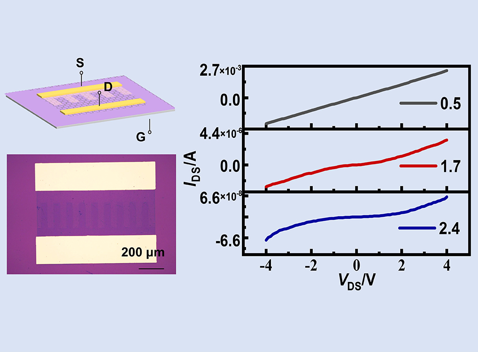
石墨烯具有优异的物理特性,如单原子厚度、极高的载流子迁移率等。然而,其零带隙的半金属特性限制了其在高性能场效应晶体管中的应用。为此,研究者们提出了石墨烯纳米化、外场诱导、掺杂以及化学图案化等策略,以调控其带隙宽度。但是,这些方法的可控性以及稳定性还需要进一步改善。在本研究中,我们提出采用电化学溴化并结合光刻图案化调控单层石墨烯的电子传输特性,通过这种方法,成功制备了图案化的溴化石墨烯(SLGBr)。进一步研究表明,单层石墨烯的电子传输性能可以通过溴化程度来调控。当溴化程度较小时,SLGBr表现为电阻特性,且其电导随溴化程度增加而减小;当溴化程度增加到一定值时,SLGBr表现为与半导体类似的特性。本研究将为全石墨烯器件的制备提供可行的技术路线,拓展其在微电子领域的应用。
崔苗苗 , 韩联欢 , 曾兰平 , 郭佳瑶 , 宋维英 , 刘川 , 吴元菲 , 罗世翊 , 刘云华 , 詹东平 . 单层石墨烯微米尺度图案化和功能化:调控电子传输特性[J]. 电化学, 2024 , 30(3) : 2305251 . DOI: 10.13208/j.electrochem.2305251
As a promising 2D material, graphene exhibits excellent physical properties including single-atom-scale thickness and remarkably high charge carrier mobility. However, its semi-metallic nature with a zero bandgap poses challenges for its application in high-performance field-effect transistors (FETs). In order to overcome these limitations, various approaches have been explored to modulate graphene's bandgap, including nanoscale confinement, external field induction, doping, and chemical micropatterning. Nevertheless, the stability and controllability still need to be improved. In this study, we propose a feasible method that combines electrochemical bromination and photolithography to precisely tune the electron transport properties of single layer graphene (SLG). Through this method, we successfully fabricated various brominated SLG (SLGBr) micropatterns with high accuracy. Futher investigation revealed that the electron transport properties of SLG can be conveniently tuned by controlling the degree of bromination. The SLGBr exhibited a resistance, and have a decreasing conductance with the bromination degree increasing. When the bromination degree increased to a critical value, the SLGBr demonstrated semiconducting characteristics. This research offers a prospective route for the fabrication of graphene-based devices, providing potential applications in the realm of microelectronics.
[1] | Kaplan A, Yuan Z, Benck J D, Govind R A, Chu X S, Wang Q H, Strano M S. Current and future directions in electron transfer chemistry of graphene[J]. Chem. Soc. Rev., 2017, 46(15): 4530-4571. |
[2] | Morozov S V, Novoselov K S, Katsnelson M I, Schedin F, Elias D C, Jaszczak J A, Geim A K. Giant intrinsic carrier mobilities in graphene and its bilayer[J]. Phys. Rev. Lett., 2008, 100(1): 016602. |
[3] | Nair R R, Blake P, Grigorenko A N, Novoselov K S, Booth T J, Stauber T, Peres N M, Geim A K. Fine structure constant defines visual transparency of graphene[J]. Science, 2008, 320(5881): 1308. |
[4] | Nan H Y, Ni Z H, Wang J, Zafar Z, Shi Z X, Wang Y Y. The thermal stability of graphene in air investigated by Raman spectroscopy[J]. J. Raman Spectrosc., 2013, 44(7): 1018-1021. |
[5] | He Q Y, Wu S X, Yin Z Y, Zhang H. Graphene-based electronic sensors[J]. Chem. Sci., 2012, 3(6): 1764-1772. |
[6] | Biro L P, Nemes-Incze P, Lambin P. Graphene: Nanoscale processing and recent applications[J]. Nanoscale, 2012, 4(6): 1824-1839. |
[7] | Schwierz F, Pezoldt J, Granzner R. Two-dimensional materials and their prospects in transistor electronics[J]. Nanoscale, 2015, 7(18): 8261-8283. |
[8] | Wei T, Bao L, Hauke F, Hirsch A. Recent advances in graphene patterning[J]. Chempluschem, 2020, 85(8): 1655-1668. |
[9] | Wei T, Hauke F, Hirsch A. Evolution of graphene patterning: From dimension regulation to molecular engineering[J]. Adv. Mater., 2021, 33(45): 2104060. |
[10] | Zheng Y Q, Wang H, Hou S F, Xia D Y. Lithographically defined graphene patterns[J]. Adv. Mater. Technol., 2017, 2(5): 1600237 |
[11] | Park J U, Nam S, Lee M S, Lieber C M. Synthesis of monolithic graphene-graphite integrated electronics[J]. Nat. Mater., 2011, 11(2): 120-125. |
[12] | Choi J K, Kwak J, Park S D, Yun H D, Kim S Y, Jung M, Kim S Y, Park K, Kang S, Kim S D, Park D Y, Lee D S, Hong S K, Shin H J, Kwon S Y. Growth of wrinkle-free graphene on texture-controlled platinum films and thermal-assisted transfer of large-scale patterned graphene[J]. ACS Nano, 2015, 9(1): 679-686. |
[13] | Zhou X B, Qi Y, Shi J P, Niu J J, Liu M X, Zhang G H, Li Q C, Zhang Z P, Hong M, Ji Q Q, Zhang Y, Liu Z F, Wu X S, Zhang Y F. Modulating the electronic properties of monolayer graphene using a periodic quasi-one-dimensional potential generated by hex-reconstructed Au(001)[J]. ACS Nano, 2016, 10(8): 7550-7557. |
[14] | Zhang Y, Tang T T, Girit C, Hao Z, Martin M C, Zettl A, Crommie M F, Shen Y R, Wang F. Direct observation of a widely tunable bandgap in bilayer graphene[J]. Nature, 2009, 459(7248): 820-823. |
[15] | Balog R, J?rgensen B, Nilsson L, Andersen M, Rienks E, Bianchi M, Fanetti M, L?gsgaard E, Baraldi A, Lizzit S, Sljivancanin Z, Besenbacher F, Hammer B, Pedersen T G, Hofmann P, Hornek?r L. Bandgap opening in graphene induced by patterned hydrogen adsorption[J]. Nat. Mater., 2010, 9(4): 315-319. |
[16] | Wu J, Xie L M, Li Y G, Wang H L, Ouyang Y J, Guo J, Dai H J. Controlled chlorine plasma reaction for noninvasive graphene doping[J]. J. Am. Chem. Soc., 2011, 133(49): 19668-19671. |
[17] | Yavari F, Kritzinger C, Gaire C, Song L, Gulapalli H, Borca-Tasciuc T, Ajayan P M, Koratkar N. Tunable bandgap in graphene by the controlled adsorption of water molecules[J]. Small, 2010, 6(22): 2535-2538. |
[18] | Elias D C, Nair R R, Mohiuddin T M, Morozov S V, Blake P, Halsall M P, Ferrari A C, Boukhvalov D W, Katsnelson M I, Geim A K, Novoselov K S. Control of graphene's properties by reversible hydrogenation: Evidence for graphane[J]. Science, 2009, 323(5914): 610-613. |
[19] | Wei T, Kohring M, Chen M, Yang S, Weber H B, Hauke F, Hirsch A. Highly efficient and reversible covalent patterning of graphene: 2D-management of chemical information[J]. Angew. Chem. Int. Ed. Engl., 2020, 59(14): 5602-5606. |
[20] | Zeng L P, Song W Y, Jin X F, He Q F, Han L H, Wu Y F, Lagrost C, Leroux Y, Hapiot P, Cao Y, Cheng J, Zhan D P. Electrochemical regulation of the band gap of single layer graphene: From semimetal to semiconductor[J]. Chem. Sci., 2023, 14(17): 4500-4505. |
[21] | Chen D H, Lin Z, Sartin M M, Huang T X, Liu J, Zhang Q G, Han L H, Li J F, Tian Z Q, Zhan D P. Photosynergetic electrochemical synthesis of graphene oxide[J]. J. Am. Chem. Soc., 2020, 142(14): 6516-6520. |
[22] | Zhong J H, Zhang J, Jin X, Liu J Y, Li Q, Li M H, Cai W, Wu D Y, Zhan D, Ren B. Quantitative correlation between defect density and heterogeneous electron transfer rate of single layer graphene[J]. J. Am. Chem. Soc., 2014, 136(47): 16609-16617. |
[23] | Ferrari A C, Basko D M. Raman spectroscopy as a versatile tool for studying the properties of graphene[J]. Nat. Nanotechnol., 2013, 8(4): 235-246. |
[24] | Li W, Li Y Q, Xu K. Facile, electrochemical chlorination of graphene from an aqueous nacl solution[J]. Nano Lett., 2021, 21(2): 1150-1155. |
[25] | Eckmann A, Felten A, Mishchenko A, Britnell L, Krupke R, Novoselov K S, Casiraghi C. Probing the nature of defects in graphene by Raman spectroscopy[J]. Nano Lett., 2012, 12(8): 3925-3930. |
[26] | Li B, Zhou L, Wu D, Peng H L, Yan K, Zhou Y, Liu Z F. Photochemical chlorination of graphene[J]. ACS Nano, 2011, 5(7): 5957-5961. |
/
〈 |
|
〉 |