光电流谱、光致发光光谱和紫外可见吸收光谱在纳米半导体光电器件研究中的联用
收稿日期: 2020-07-28
修回日期: 2020-08-04
网络出版日期: 2020-08-25
基金资助
国家自然科学基金项目(21533006);国家自然科学基金项目(21273182);国家重点研发计划(2018YFC1602805)
Combined Applications of Photocurrent Spectroscopy, Photoluminescence Spectroscopy and UV-Vis Spectroscopy for Nano-Semiconductor Based Photoelectric Devices
Received date: 2020-07-28
Revised date: 2020-08-04
Online published: 2020-08-25
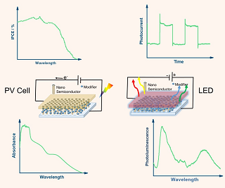
在纳米半导体中由于纳米效应(如量子尺寸效应),其电子结构与块体半导体有所不同。进一步地,当纳米半导体与基底和其他组分结合制成器件后,其性质又受到基底或其他组分的影响,这两点导致了基于纳米半导体的光电器件的性能以及相应表征方法也大不相同。将光电流谱、光致发光光谱和紫外可见吸收光谱三种技术有机地结合起来,可以更好地表征纳米半导体的电子性质和光电性能。本文根据纳米半导体材料与电极的电子性质特点及其测量,结合本课题组前期工作,举例介绍三种谱学方法相结合应用于探究光伏电池和电致发光器件的纳米半导体材料的性能,以及纳米半导体材料表面态的表征。
卞斯达 , 周剑章 , 林仲华 . 光电流谱、光致发光光谱和紫外可见吸收光谱在纳米半导体光电器件研究中的联用[J]. 电化学, 2021 , 27(1) : 45 -55 . DOI: 10.13208/j.electrochem.200728
The electronic structures and properties of nano-semiconductors are quite different from those of bulk semiconductors due to the nano-size effect (such as quantum size effect). Moreover, when the nano-semiconductor materials are deposited onto the substrate to construct a device, their electronic properties are also affected by the substrate or other components, which may lead to different performances of nano-semiconductors based photoelectric devices, and consequently, different corresponding characterization methods are needed. The combination of photocurrent spectroscopy, photoluminescence spectroscopy with UV-Vis absorption spectroscopy can provide a more comprehensive characterization for the electronic properties and photoelectrochemical performances of nano-semiconductors in photoelectric devices. Our research group has long devoted to the studies in the preparations and characterizations of different nano-semiconductors for photoelectric devices. In this review, we firstly introduce the main different features in electronic properties of nano-semiconductors and the corresponding characterization methods, and then describe how to combine the abovementioned three spectroscopic methods to investigate the electronic properties and photoelectrochemical performances of the nano-semiconductors for photovoltaic cells, electroluminescent diodes, and other photocatalytic systems by detailed examples. Photoluminescence spectroscopy is a common method to characterize the surface states of the semiconductors, while photocurrent spectroscopy can provide the supplementary information of surface states. Especially, the photoluminescence efficiency is low for the nonradiactive recombination dominated materials such as indirect-bandgap semiconductors. The results of photocurrent spectroscopy are more useful under these circumstances. Furthermore, the combined characterization in surface states of the nano-semiconductors by photocurrent spectroscopy with photoluminescence spectroscopy is specially discussed. The combined applications of these three spectroscopic methods for the nano-semiconductors in photoeltric devices are not only beneficial to obtain intensive understanding the electric properties and the photo-induced charge transfer mechanism at the interface of the nano-semiconductors, but also useful to guide the preparation of nano-semiconductor materials for photoelectric devices and optimal to the photoelectrochemical performances.
[1] | Jackson H E, Smith L M. Chapter two - Optical properties of semiconductor nanowires: insights into band structure and carrier dynamics[M]// Semiconductors and Semimetals Elsevier, 2016,94:17-74. |
[2] | Wojtyla S, Baran T. Photosensitization and photocurrent switching effects in wide band gap semiconductors: CuI and TiO2 functionalized with iron and nickel complexes: from semiconductors to logic devices[J]. J. Inorg. Organomet. Poly. Mater., 2017,27(2):436-445. |
[3] | Gfroerer T H. Photoluminescence in analysis of surfaces and interfaces[M]. Chichester: John Wiley & Sons Ltd, 2006: 1-2. |
[4] | Wang F, Liu X K, Gao F. Chapter 1-Fundamentals of solar cells and light-emitting diodes[M]// Advanced nanomaterials for solar cells and light emitting diodes, Amsterdam: Elsevier, 2019: 1-35. |
[5] | Maku?a P, Pacia M, Macyk W. How to correctly determine the band gap energy of modified semiconductor photocatalysts based on UV-vis spectra[J]. J. Phys. Chem. Lett., 2018,9(23):6814-6817. |
[6] | Kozio? R, ?apiński M, Syty P, Koszelow D, Sadowski W, Sienkiewicz J E, Koscielska B. Evolution of Ag nanostructures created from thin films: UV-vis absorption and its theoretical predictions[J]. Beilstein J. Nanotechnol., 2020,11:494-507. |
[7] | Hagfeldt A, Graetzel M. Light-induced redox reactions in nanocrystalline systems[J]. Chem. Rev., 1995,95(1):49-68. |
[8] | Brus L E. Electron-electron and electron-hole interactions in small semiconductor crystallites: The size dependence of the lowest excited electronic state[J]. J. Chem. Phys., 1984,80(9):4403-4409. |
[9] | Tauc J, Grigorovici R, Vancu A. Optical properties and electronic structure of amorphous germanium[J]. Phys. Stat. Sol. (b), 1966,15(2):627-637. |
[10] | Kubelka P, Munk F. A Contribution to the optics of pigments[J]. J. Techn. Phys., 1931, (12):593-599. |
[11] | G?rtner W W. Depletion-layer photoeffects in semiconductors[J]. Phys. Rev., 1959,116(1):84-87. |
[12] | Canham L T. Silicon quantum wire array fabrication by electrochemical and chemical dissolution of wafers[J]. Appl. Phys. Lett., 1990,57(10):1046-1048. |
[13] | Feng Z F, Zhang Q B, Lin L L, Quo H H, Zhou J Z, Lin Z H. <0001>-preferential growth of cdse nanowires on conducting glass: Template-free electrodeposition and application in photovoltaics[J]. Chem. Mater., 2010,22(9):2705-2710. |
[14] | Yuhas B D, Yang P. Nanowire-based all-oxide solar cells[J]. J. Am. Chem. Soc., 2009,131(10):3756-3761. |
[15] | Jiang Q L, Sheng X, Li Y X, Feng X J, Xu T. Rutile TiO2 nanowire-based perovskite solar cells[J]. Chem. Commun., 2014,50(94):14720-14723. |
[16] | Consonni V, Briscoe J, K?rber E, Li X, Cossuet T. ZnO nanowires for solar cells: a comprehensive review[J]. Nanotechnology, 2019,30(36):362001. |
[17] | Yang X, Li H, Zhang W, Sun M X, Li L Q, Xu N, Wu J D, Sun J. High visible photoelectrochemical activity of Ag nanoparticle-sandwiched CdS/Ag/ZnO nanorods[J]. ACS Appl. Mater. Inter., 2017,9(1):658-667. |
[18] | Lam K T, Hsiao Y J, Ji L W, Fang T H, Hsiao K H, Chu T T. High-sensitive ultraviolet photodetectors based on ZnO nanorods/CdS heterostructures[J]. Nanoscale Res. Lett., 2017,12(1):31. |
[19] | Sheng P T, Yao L, Yang P, Yang D F, Lu C K, Cao K S, Li W L. The origin of enhanced photoelectrochemical activity in metal-ion-doped ZnO/CdS quantum dots[J]. J. Alloy. Compd., 2020,822:153700. |
[20] | Ben Taieb S, Pham Truong T N, Chaguetmi S, Ben Naceur J, Bardaoui A, Gannouni M, Decorse P, Mouton L, Nowak S, Mammeri F, Chtourou R, Ammar S. An easy-to achieve approach for the fabrication of CdS QDs sensitized TiO2 nanotubes and their enhanced photoelectrochemical performance[J]. J. Photochem. Photobiol.-Chem., 2017,332:337-344. |
[21] | Zhang Q B(张桥保), Feng Z F(冯增芳), Han N N(韩楠楠). Preparation and photoeletrochemical performance of CdS quantum dot sensitized ZnO nanorod array electrodes[J]. Acta Phys.-Chem. Sin. (物理化学学报), 2010,26(11):2927-2934. |
[22] | Lu J F, Zhu Q X, Zhu Z, Liu Y J, Wei M, Shi Z L, Xu C X. Plasmon-mediated exciton-phonon coupling in a ZnO microtower cavity[J]. J. Mater. Chem. C, 2016,4(33):7718-7723. |
[23] | Wang J J, Wu X J, He Y H, Guo W, Zhang Q H, Wang Y, Wang Z H. Investigation of the electronic structure of CdS nanoparticles with sum frequency generation and photoluminescence spectroscopy[J]. J. Phys. Chem. C, 2019,123(45):27712-27716. |
[24] | Wang Z L. Splendid one-dimensional nanostructures of zinc oxide: A new nanomaterial family for nanotechnology[J]. ACS Nano, 2008,2(10):1987-1992. |
[25] | Voss T, Waldvogel S R. Hybrid LEDs based on ZnO nanowire structures[J]. Mat. Sci. Semicon. Proc., 2017,69:52-56. |
[26] | Qiao S, Liu J H, Fu G S, Ren K L, Li Z Q, Wang S F, Pan C F. ZnO nanowire based CIGS solar cell and its efficiency enhancement by the piezo-phototronic effect[J]. Nano Energy, 2018,49:508-514. |
[27] | Guo H H, Lin Z H, Feng Z F, Lin L L, Zhou J Z. White-light-emitting diode based on ZnO nanotubes[J]. J. Phys. Chem. C, 2009,113(28):12546-12550. |
[28] | Peng W Q, Qu S C, Cong G W, Wang Z G. Synjournal and structures of morphology-controlled ZnO nano- and microcrystals[J]. Cryst. Growth Des., 2006,6(6):1518-1522. |
[29] | Xu L F, Liao Q, Zhang J P, Ai X C, Xu D S. Single-crystalline ZnO nanotube arrays on conductive glass substrates by selective disolution of electrodeposited ZnO nanorods[J]. J. Phys. Chem. C, 2007,111(12):4549-4552. |
[30] | Van Dijken A, Meulenkamp E A, Vanmaekelbergh D, Meijerink A. emission[J]. J. Lumines., 2000, 87-89:454-456. |
[31] | Zhang Q B, Guo H H, Feng Z F, Lin L L, Zhou J Z, Lin Z H. n-ZnO nanorods/p-CuSCN heterojunction light-emitting diodes fabricated by electrochemical method[J]. Electrochim. Acta, 2010,55(17):4889-4894. |
[32] | Zheng J W, Mo L E, Chen W C, Jiang L, Ding Y, Li Z Q, Hu L H, Dai S Y. Surface states in TiO2 submicrosphere films and their effect on electron transport[J]. Nano Res., 2017,10(11):3671-3679. |
[33] | Sachs M, Pastor E, Kafizas A, Durrant J R. Evaluation of surface state mediated charge recombination in anatase and rutile TiO2[J]. J. Phys. Chem. Lett., 2016,7(19):3742-3746. |
[34] | Zawadzki P, Laursen A B, Jacobsen K W, Dahl S. Oxidative trends of TiO2—hole trapping at anatase and rutile surfaces[J]. Energy Environ. Sci., 2012,5(12):9866-9869. |
[35] | Gao C, Peng Y Q, Hu L H, Mo L E, Zhang X X, Hayat T, Alsaedi A, Dai S Y. A comparative study of the density of surface states in solid and hollow TiO2 microspheres[J]. Inorg. Chem. Front., 2018,5(9):2284-2290. |
[36] | Sudhagar P, Devadoss A, Nakata K, Terashima C, Fujishima A. Enhanced photoelectrocatalytic water splitting at hierarchical Gd3+:TiO2 nanostructures through amplifying light reception and surface states passivation[J]. J. Electrochem. Soc., 2014,162(3):H108-H114. |
[37] | Guo Q, Zhou C Y, Ma Z B, Yang X M. Fundamentals of TiO2 photocatalysis: Concepts, mechanisms, and challenges[J]. Adv. Mater., 2019,31(50):1901997. |
[38] | Clavero C. Plasmon-induced hot-electron generation at nanoparticle/metal-oxide interfaces for photovoltaic and photocatalytic devices[J]. Nat. Photonics, 2014,8(2):95-103. |
[39] | Linic S, Christopher P, Ingram D B. Plasmonic-metal nano-structures for efficient conversion of solar to chemical energy[J]. Nat. Mater., 2011,10(12):911-921. |
[40] | Liu Z, Hou W, Pavaskar P, Aykol M, Cronin S B. Plasmon resonant enhancement of photocatalytic water splitting under visible illumination[J]. Nano Lett., 2011,11(3):1111-1116. |
[41] | Liu E Z, Kang L M, Wu F, Sun T, Hu X Y, Yang Y H, Liu H C, Fan J. Photocatalytic reduction of CO2 into methanol over Ag/TiO2 nanocomposites enhanced by surface plasmon resonance[J]. Plasmonics, 2014,9(1):61-70. |
[42] | Bian S D(卞斯达). Spectroscopic and photoelectrochemical characterizations of plasmon photocatalytic reaction in Ag-TiO2 nanocomposites[D]. Xiamen University (厦门大学), 2020. |
[43] | Varma R S, Thorat N, Fernandes R, Kothari D C, Patel N, Miotello A. Dependence of photocatalysis on charge carrier separation in Ag-doped and decorated TiO2 nano-composites[J]. Catal. Sci. Technol., 2016,6(24):8428-8440. |
[44] | Ge M Z, Cao C Y, Li S H, Tang Y X, Wang L N, Qi N, Huang J Y, Zhang K Q, Al-Deyab S S, Lai Y K. In situ plasmonic Ag nanoparticle anchored TiO2 nanotube arrays as visible-light-driven photocatalysts for enhanced water splitting[J]. Nanoscale, 2016,8(9):5226-5234. |
/
〈 |
|
〉 |