
电化学(中英文) ›› 2021, Vol. 27 ›› Issue (1): 45-55. doi: 10.13208/j.electrochem.200728
卞斯达, 周剑章*( ), 林仲华
收稿日期:2020-07-28
修回日期:2020-08-04
出版日期:2021-02-28
发布日期:2020-08-25
通讯作者:
周剑章
E-mail:jzzhou@xmu.edu.cn
基金资助:
Si-Da Bian, Jian-Zhang Zhou*(), Zhong-Hua Lin
Received:2020-07-28
Revised:2020-08-04
Published:2021-02-28
Online:2020-08-25
Contact:
Jian-Zhang Zhou
E-mail:jzzhou@xmu.edu.cn
摘要:
在纳米半导体中由于纳米效应(如量子尺寸效应),其电子结构与块体半导体有所不同。进一步地,当纳米半导体与基底和其他组分结合制成器件后,其性质又受到基底或其他组分的影响,这两点导致了基于纳米半导体的光电器件的性能以及相应表征方法也大不相同。将光电流谱、光致发光光谱和紫外可见吸收光谱三种技术有机地结合起来,可以更好地表征纳米半导体的电子性质和光电性能。本文根据纳米半导体材料与电极的电子性质特点及其测量,结合本课题组前期工作,举例介绍三种谱学方法相结合应用于探究光伏电池和电致发光器件的纳米半导体材料的性能,以及纳米半导体材料表面态的表征。
卞斯达, 周剑章, 林仲华. 光电流谱、光致发光光谱和紫外可见吸收光谱在纳米半导体光电器件研究中的联用[J]. 电化学(中英文), 2021, 27(1): 45-55.
Si-Da Bian, Jian-Zhang Zhou, Zhong-Hua Lin. Combined Applications of Photocurrent Spectroscopy, Photoluminescence Spectroscopy and UV-Vis Spectroscopy for Nano-Semiconductor Based Photoelectric Devices[J]. Journal of Electrochemistry, 2021, 27(1): 45-55.

图1
以ECD、SLS合成的CdSe纳米线以及CdSe纳米粒子组装的光伏电池的(A)光电流密度-电压谱图;(B) IPCE谱;(C) 紫外可见吸收光谱;(D) 光致发光光谱 (激发光波长:325 nm),光伏电池的有效面积为1 cm2[13]。(网络版彩图)
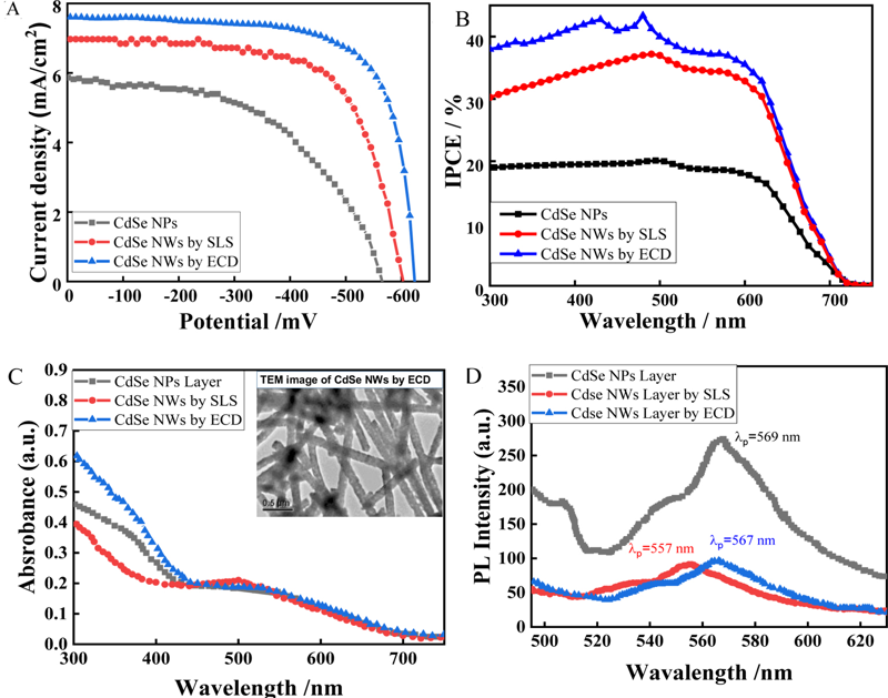
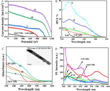
图2
单纯CdS量子点电极和单纯ZnO纳米棒阵列电极及不同CdS沉积次数下得到的CdS量子点敏化ZnO纳米棒薄膜复合电极的(A)光电流密度-电压谱图;(B) IPCE谱;(C) 紫外可见吸收光谱图;(D) 光致发光光谱图(激发波长320 nm),电极有效面积:0.1 cm2[21]。(网络版彩图)
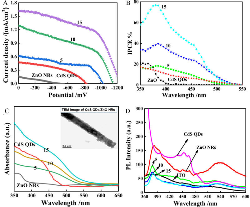
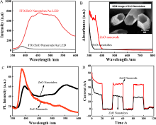
图3
ZnO纳米管和ZnO纳米棒(A)组装的二极管在25 V下的电致发光谱图;(B) 紫外可见吸收光谱;(C)光致发光光谱(激发光波长为320 nm);(D) 在340 nm光下的光电流响应,施加电位:0.2 V (vs. SCE)[27]。(网络版彩图)

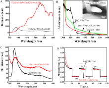
图4
ZnO纳米棒以及ZnO纳米棒/CuSCN复合膜的(A)组装的二极管在25 V下的电致发光谱图;(B)紫外可见吸收光谱;(C)光致发光光谱 (激发波长:340 nm);(D)在340 nm光下的光电流响应,施加电位:0 V (vs. SCE)[31]。(网络版彩图)
图5
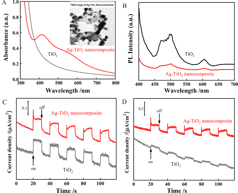
TiO2和Ag-TiO2复合体系: (A) 紫外可见吸收光谱;(B) 光致发光光谱(激发波长:380 nm);(C) 在385 ~ 390 nm光下的光电流响应,施加电位:0.3 V (vs. Ag/AgCl(sat. KCl));(D) 460 ~ 470 nm光下的光电流响应,施加电位: 0.3 V (vs. Ag/AgCl(sat. KCl))。(网络版彩图)
| [1] | Jackson H E, Smith L M. Chapter two - Optical properties of semiconductor nanowires: insights into band structure and carrier dynamics[M]// Semiconductors and Semimetals Elsevier, 2016,94:17-74. |
| [2] |
Wojtyla S, Baran T. Photosensitization and photocurrent switching effects in wide band gap semiconductors: CuI and TiO2 functionalized with iron and nickel complexes: from semiconductors to logic devices[J]. J. Inorg. Organomet. Poly. Mater., 2017,27(2):436-445.
doi: 10.1007/s10904-016-0484-6 URL |
| [3] | Gfroerer T H. Photoluminescence in analysis of surfaces and interfaces[M]. Chichester: John Wiley & Sons Ltd, 2006: 1-2. |
| [4] | Wang F, Liu X K, Gao F. Chapter 1-Fundamentals of solar cells and light-emitting diodes[M]// Advanced nanomaterials for solar cells and light emitting diodes, Amsterdam: Elsevier, 2019: 1-35. |
| [5] |
Makuła P, Pacia M, Macyk W. How to correctly determine the band gap energy of modified semiconductor photocatalysts based on UV-vis spectra[J]. J. Phys. Chem. Lett., 2018,9(23):6814-6817.
doi: 10.1021/acs.jpclett.8b02892 URL pmid: 30990726 |
| [6] |
Kozioł R, Łapiński M, Syty P, Koszelow D, Sadowski W, Sienkiewicz J E, Koscielska B. Evolution of Ag nanostructures created from thin films: UV-vis absorption and its theoretical predictions[J]. Beilstein J. Nanotechnol., 2020,11:494-507.
URL pmid: 32274288 |
| [7] |
Hagfeldt A, Graetzel M. Light-induced redox reactions in nanocrystalline systems[J]. Chem. Rev., 1995,95(1):49-68.
doi: 10.1021/cr00033a003 URL |
| [8] |
Brus L E. Electron-electron and electron-hole interactions in small semiconductor crystallites: The size dependence of the lowest excited electronic state[J]. J. Chem. Phys., 1984,80(9):4403-4409.
doi: 10.1063/1.447218 URL |
| [9] |
Tauc J, Grigorovici R, Vancu A. Optical properties and electronic structure of amorphous germanium[J]. Phys. Stat. Sol. (b), 1966,15(2):627-637.
doi: 10.1002/(ISSN)1521-3951 URL |
| [10] | Kubelka P, Munk F. A Contribution to the optics of pigments[J]. J. Techn. Phys., 1931, (12):593-599. |
| [11] |
Gärtner W W. Depletion-layer photoeffects in semiconductors[J]. Phys. Rev., 1959,116(1):84-87.
doi: 10.1103/PhysRev.116.84 URL |
| [12] |
Canham L T. Silicon quantum wire array fabrication by electrochemical and chemical dissolution of wafers[J]. Appl. Phys. Lett., 1990,57(10):1046-1048.
doi: 10.1063/1.103561 URL |
| [13] |
Feng Z F, Zhang Q B, Lin L L, Quo H H, Zhou J Z, Lin Z H. <0001>-preferential growth of cdse nanowires on conducting glass: Template-free electrodeposition and application in photovoltaics[J]. Chem. Mater., 2010,22(9):2705-2710.
doi: 10.1021/cm901703d URL |
| [14] |
Yuhas B D, Yang P. Nanowire-based all-oxide solar cells[J]. J. Am. Chem. Soc., 2009,131(10):3756-3761.
URL pmid: 19275263 |
| [15] |
Jiang Q L, Sheng X, Li Y X, Feng X J, Xu T. Rutile TiO2 nanowire-based perovskite solar cells[J]. Chem. Commun., 2014,50(94):14720-14723.
doi: 10.1039/C4CC07367C URL |
| [16] |
Consonni V, Briscoe J, Kärber E, Li X, Cossuet T. ZnO nanowires for solar cells: a comprehensive review[J]. Nanotechnology, 2019,30(36):362001.
doi: 10.1088/1361-6528/ab1f2e URL pmid: 31051478 |
| [17] |
Yang X, Li H, Zhang W, Sun M X, Li L Q, Xu N, Wu J D, Sun J. High visible photoelectrochemical activity of Ag nanoparticle-sandwiched CdS/Ag/ZnO nanorods[J]. ACS Appl. Mater. Inter., 2017,9(1):658-667.
doi: 10.1021/acsami.6b12259 URL |
| [18] |
Lam K T, Hsiao Y J, Ji L W, Fang T H, Hsiao K H, Chu T T. High-sensitive ultraviolet photodetectors based on ZnO nanorods/CdS heterostructures[J]. Nanoscale Res. Lett., 2017,12(1):31.
doi: 10.1186/s11671-016-1818-6 URL |
| [19] |
Sheng P T, Yao L, Yang P, Yang D F, Lu C K, Cao K S, Li W L. The origin of enhanced photoelectrochemical activity in metal-ion-doped ZnO/CdS quantum dots[J]. J. Alloy. Compd., 2020,822:153700.
doi: 10.1016/j.jallcom.2020.153700 URL |
| [20] |
Ben Taieb S, Pham Truong T N, Chaguetmi S, Ben Naceur J, Bardaoui A, Gannouni M, Decorse P, Mouton L, Nowak S, Mammeri F, Chtourou R, Ammar S. An easy-to achieve approach for the fabrication of CdS QDs sensitized TiO2 nanotubes and their enhanced photoelectrochemical performance[J]. J. Photochem. Photobiol.-Chem., 2017,332:337-344.
doi: 10.1016/j.jphotochem.2016.09.001 URL |
| [21] |
Zhang Q B(张桥保), Feng Z F(冯增芳), Han N N(韩楠楠). Preparation and photoeletrochemical performance of CdS quantum dot sensitized ZnO nanorod array electrodes[J]. Acta Phys.-Chem. Sin. (物理化学学报), 2010,26(11):2927-2934.
doi: 10.3866/PKU.WHXB20101113 URL |
| [22] |
Lu J F, Zhu Q X, Zhu Z, Liu Y J, Wei M, Shi Z L, Xu C X. Plasmon-mediated exciton-phonon coupling in a ZnO microtower cavity[J]. J. Mater. Chem. C, 2016,4(33):7718-7723.
doi: 10.1039/C6TC02288J URL |
| [23] |
Wang J J, Wu X J, He Y H, Guo W, Zhang Q H, Wang Y, Wang Z H. Investigation of the electronic structure of CdS nanoparticles with sum frequency generation and photoluminescence spectroscopy[J]. J. Phys. Chem. C, 2019,123(45):27712-27716.
doi: 10.1021/acs.jpcc.9b09750 URL |
| [24] |
Wang Z L. Splendid one-dimensional nanostructures of zinc oxide: A new nanomaterial family for nanotechnology[J]. ACS Nano, 2008,2(10):1987-1992.
URL pmid: 19206442 |
| [25] |
Voss T, Waldvogel S R. Hybrid LEDs based on ZnO nanowire structures[J]. Mat. Sci. Semicon. Proc., 2017,69:52-56.
doi: 10.1016/j.mssp.2016.11.027 URL |
| [26] |
Qiao S, Liu J H, Fu G S, Ren K L, Li Z Q, Wang S F, Pan C F. ZnO nanowire based CIGS solar cell and its efficiency enhancement by the piezo-phototronic effect[J]. Nano Energy, 2018,49:508-514.
doi: 10.1016/j.nanoen.2018.04.070 URL |
| [27] |
Guo H H, Lin Z H, Feng Z F, Lin L L, Zhou J Z. White-light-emitting diode based on ZnO nanotubes[J]. J. Phys. Chem. C, 2009,113(28):12546-12550.
doi: 10.1021/jp902607c URL |
| [28] |
Peng W Q, Qu S C, Cong G W, Wang Z G. Synjournal and structures of morphology-controlled ZnO nano- and microcrystals[J]. Cryst. Growth Des., 2006,6(6):1518-1522.
doi: 10.1021/cg0505261 URL |
| [29] |
Xu L F, Liao Q, Zhang J P, Ai X C, Xu D S. Single-crystalline ZnO nanotube arrays on conductive glass substrates by selective disolution of electrodeposited ZnO nanorods[J]. J. Phys. Chem. C, 2007,111(12):4549-4552.
doi: 10.1021/jp068485m URL |
| [30] |
Van Dijken A, Meulenkamp E A, Vanmaekelbergh D, Meijerink A. emission[J]. J. Lumines., 2000, 87-89:454-456.
doi: 10.1016/S0022-2313(99)00482-2 URL |
| [31] |
Zhang Q B, Guo H H, Feng Z F, Lin L L, Zhou J Z, Lin Z H. n-ZnO nanorods/p-CuSCN heterojunction light-emitting diodes fabricated by electrochemical method[J]. Electrochim. Acta, 2010,55(17):4889-4894.
doi: 10.1016/j.electacta.2010.03.082 URL |
| [32] |
Zheng J W, Mo L E, Chen W C, Jiang L, Ding Y, Li Z Q, Hu L H, Dai S Y. Surface states in TiO2 submicrosphere films and their effect on electron transport[J]. Nano Res., 2017,10(11):3671-3679.
doi: 10.1007/s12274-017-1577-4 URL |
| [33] |
Sachs M, Pastor E, Kafizas A, Durrant J R. Evaluation of surface state mediated charge recombination in anatase and rutile TiO2[J]. J. Phys. Chem. Lett., 2016,7(19):3742-3746.
doi: 10.1021/acs.jpclett.6b01501 URL pmid: 27564137 |
| [34] |
Zawadzki P, Laursen A B, Jacobsen K W, Dahl S. Oxidative trends of TiO2—hole trapping at anatase and rutile surfaces[J]. Energy Environ. Sci., 2012,5(12):9866-9869.
doi: 10.1039/c2ee22721e URL |
| [35] |
Gao C, Peng Y Q, Hu L H, Mo L E, Zhang X X, Hayat T, Alsaedi A, Dai S Y. A comparative study of the density of surface states in solid and hollow TiO2 microspheres[J]. Inorg. Chem. Front., 2018,5(9):2284-2290.
doi: 10.1039/C8QI00633D URL |
| [36] |
Sudhagar P, Devadoss A, Nakata K, Terashima C, Fujishima A. Enhanced photoelectrocatalytic water splitting at hierarchical Gd3+:TiO2 nanostructures through amplifying light reception and surface states passivation[J]. J. Electrochem. Soc., 2014,162(3):H108-H114.
doi: 10.1149/2.0161503jes URL |
| [37] |
Guo Q, Zhou C Y, Ma Z B, Yang X M. Fundamentals of TiO2 photocatalysis: Concepts, mechanisms, and challenges[J]. Adv. Mater., 2019,31(50):1901997.
doi: 10.1002/adma.v31.50 URL |
| [38] |
Clavero C. Plasmon-induced hot-electron generation at nanoparticle/metal-oxide interfaces for photovoltaic and photocatalytic devices[J]. Nat. Photonics, 2014,8(2):95-103.
doi: 10.1038/nphoton.2013.238 URL |
| [39] |
Linic S, Christopher P, Ingram D B. Plasmonic-metal nano-structures for efficient conversion of solar to chemical energy[J]. Nat. Mater., 2011,10(12):911-921.
URL pmid: 22109608 |
| [40] |
Liu Z, Hou W, Pavaskar P, Aykol M, Cronin S B. Plasmon resonant enhancement of photocatalytic water splitting under visible illumination[J]. Nano Lett., 2011,11(3):1111-1116.
doi: 10.1021/nl104005n URL pmid: 21319840 |
| [41] |
Liu E Z, Kang L M, Wu F, Sun T, Hu X Y, Yang Y H, Liu H C, Fan J. Photocatalytic reduction of CO2 into methanol over Ag/TiO2 nanocomposites enhanced by surface plasmon resonance[J]. Plasmonics, 2014,9(1):61-70.
doi: 10.1007/s11468-013-9598-7 URL |
| [42] | Bian S D(卞斯达). Spectroscopic and photoelectrochemical characterizations of plasmon photocatalytic reaction in Ag-TiO2 nanocomposites[D]. Xiamen University (厦门大学), 2020. |
| [43] |
Varma R S, Thorat N, Fernandes R, Kothari D C, Patel N, Miotello A. Dependence of photocatalysis on charge carrier separation in Ag-doped and decorated TiO2 nano-composites[J]. Catal. Sci. Technol., 2016,6(24):8428-8440.
doi: 10.1039/C6CY01605G URL |
| [44] |
Ge M Z, Cao C Y, Li S H, Tang Y X, Wang L N, Qi N, Huang J Y, Zhang K Q, Al-Deyab S S, Lai Y K. In situ plasmonic Ag nanoparticle anchored TiO2 nanotube arrays as visible-light-driven photocatalysts for enhanced water splitting[J]. Nanoscale, 2016,8(9):5226-5234.
doi: 10.1039/c5nr08341a URL pmid: 26878901 |
| No related articles found! |
| 阅读次数 | ||||||
|
全文 |
|
|||||
|
摘要 |
|
|||||